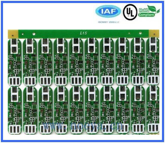
Electronics PCB board for adapter:
Technical details:
1)layer count: 2 layer
2)material details: 1mm FR-1
3)Min. Board thickness:
0.4mm for 2 layers and 4 layers
0.8mm for 6 layers
4)available finished copper weight: 0.5-4oz,
Available board thickness: 0.4mm-3.2mm
Available surface finishing: HASL, OSP, IMMERSION GOLD, gold plated, flash gold, ENIG, immersion Tin
Available soldermask: White, black, green, blue, yellow(orange), RED
5)Max board size: 600mm*600mm
6)plated gold/gold coating/flash gold/gold flash finishing
7)Min line width/spacing: 0.23mm
Min, Hole size(aperture): 0.2mm, hole tolerance: +/-0.05mm
Min. Solder bridge: 0.08mm, Dimension tolerance: +/-0.1mm
6)Outline/profile/contour: CNC Routing, milling
7)Lead time: 5 days for prototypes, 7-9 days for mass production
8)Certification: RoHS&UL
9)application: Adapter
Board size details and panelized details:
3)circuit characteristic: Simple; Board size: 156mm*20mm/panel
Panel details: Each panel with 20PCS; Breaking off strips: 2*5mm
Advantages:
1)Best quality and attractive price.
2)Best on time shipping
3)with 100%E-test
4)Customer service
5)Instant quote
6)No minimum lot Requirements
7)Ultra modern manufacturing facility
Main markets:
Brazil, Canada, Australia, Germany
Hot-selling time:
Hot selling in Feb, Mar. In 2011; Jan. And Feb in 2012
Capacity:
8, 000sqm/month for 6 layers PCB; 10, 000sqm/month for 4 layers PCB; 12, 000sqm/month for 2 layers PCB; 15, 000sqm/month for 1 layer PCB
|
NOEYA BARE PCB MANUFACTURING CAPABILITY |
|
Item |
Capability |
|
1. Base Material |
FR-4 / High TG FR-4 / 94HB/FR-1/CEM-1 |
|
2. Layers |
1-6 |
|
3. Finised inner/outer copper thickness |
1-6OZ |
|
4. Finished board thickness |
0.2-7.0mm |
|
Tolerance |
Board thickness≤ 1.0mm: +/-0.1mm |
|
1< Board thickness≤ 2.0mm: +/-10% |
|
|
|
Board thickness> 2.0mm: +/-8% |
|
5. Max panel size |
600*600mm |
|
6. Min conductor line width/spacing |
Inner layers: ≥ 3/3mil |
|
Outer layers: ≥ 3.5/3.5mil |
|
7. Min hole size |
Mechanical hole: 0.15mm |
|
Laser hole: 0.1mm |
|
Drilling precision: first drilling |
First drilling: 1mil |
|
|
|
Second drilling: 4mil |
|
8. Warpage |
Board thickness≤ 0.79mm: β ≤ 1.0% |
|
0.80≤ Board thickness≤ 2.4mm: β ≤ 0.7% |
|
Board thickness≥ 2.5mm: β ≤ 0.5% |
|
9. Controlled Impedance |
+/-5% |
|
10. Aspect Ratio |
15: 1 |
|
11. Min welding ring |
4mil |
|
12. Min solder mask bridge |
≥ 0.08mm |
|
13. Plugging vias capability |
0.2-0.8mm |
|
14. Hole tolerance |
PTH: +/-3mil |
|
NPTH: +/-2mil |
|
15. Outline profile |
Rout/ V-cut/ Bridge/ Stamp hole |
|
16. Surface treatment |
OSP: 0.5-0.5um |
|
HASL: 2-40um |
|
Lead free HASL: 2-40um |
|
ENIG: Au 1-10U’ ’ |
|
ENEPIG: PB 2-5U’ ’ / Au 1-8U’ ’ |
|
Immersion Tin: 0.8-1.2um |
|
Peelable blue, green, yellow, RED, White, black mask |
|
Carbon ink |
|
Gold plating: Au 1-150U’ ’ |
|
17. E-testing pass percent |
97% pass for the first time, +/-2%(tolerance) |
|
FQC-Physical Lab: Reliability tests |
|
18. Certificate |
ROHS UL: E159194 ISO9001: 2008 IPC SGS |
|
Our equipments |
|
1. Drilling workshop |
4 drilling bits of drilling machine: 4 sets |
|
2 drilling bits of drilling machine: 2 sets |
|
2. photo plotting workshop |
Israel “ ORBOTECH” Photo Plotters |
|
3. AOI |
AOI machine |
|
4. IPQC |
“ OXFORD” CMI 700 Copper Thickness Tester |
|
5. Impedance test |
USA “ Tektronix” DSA 8200 Impedance Tester |
|
6. Outline workshop |
CNC routing machine: 7 sets |
|
angle-cutting machine |
|
V-cut machine |
|
7. Testing Workshop |
Surpass X-600: 2sets |
|
WTD FT-2808: 5sets |
|
WTD HV300: 1set |
|
8. X-ray |
X-ray machine |
|
Acceptable file format |
|
GERBER file, PROTEL series, PADS series, POWER PCB series, AutoCAD series. |
Shenzhen Noeya Technology Co., Ltd. is a professional high-tech PCB manufacturer, which was built in 2003. Over years, our scale has been expanding: More than 300 workers, more than 1, 500m² For day-output, more than 500, 000m² For year-output.
Our main products mainly applied FR-4(TG135-170), CEM-1 and FR-1(94V0). The finished PCB boards including Single and double layer PCB, 4 layers PCB, 6 layer and 8 layer multilayer PCB, High Frequency PCB(HFPCB), HDI PCB, High density PCB with blind and buried-vias. Especially we are strong in single layer, double layer, 4 layers and 6 layers PCB board, which are widely applied in LED lightings, computers, Telecommunications, Auto, digital, home appliance and consumer electronics. Selling well both at home and abroad.
We've got a contingent of producing and sales team. With advanced processed devices and checking and testing technology. We are cooperating with much domestic and abroad branded business, like Gree, FOSS, BYD Auto and Gospell etc. We abide by the national laws and regulations, pay emphasis on environment and environmental production. We have already got ISO9001: 2000. Our products quality can meet IPC-A-600F \IPC-D-600G, MIL-STD-105D LEVEL II \and UL STANDARD. With strictly quality checking and strictly following-up the goods, supply exact lead time and quality products.
We will take a series of special training to improve our staff's professional skills and service quality and speed so that our management system can be enter into normalization and informationization.
