Product Specifications
| Prod Model: |
GaN-FS-10 |
| Markets: |
North America,South America,Eastern Europe,Southeast Asia,Africa,Oceania,Mid East,Eastern Asia,Western Europe |
| Material: |
LED |
| Type: |
Decoration |
| Suitable For: |
Children |
Product Description
Applications:
Blue LDs(405nm < 400_415nm>) can be used for high-density data storage, laser print, laser display, laser projection camera, etc.
GaN-based MQWs LDs
Short wavelength laser: Green/UV/Deep UV
Specifications:
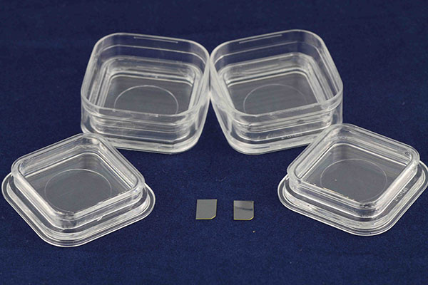
Item:GaN-FS-10
Dimensions:10.0mm×10.5mm
Marco Defect Density:LD Level > 90%
Thickness 350 ± 25 µm
Orientation C-axis(0001) ± 0.5°
TTV(Total Thickness Variation) ≤15 µm
BOW ≤20 µm
Conduction Type N-type Semi-Insulating
Resistivity(300K) < 0.5 Ωcm >106 Ωcm
Dislocation Density Less than 5x106 cm-2
Useable Surface Area > 90%
Polishing:Front Surface: Ra < 0.2nm. Epi-ready polished
Back Surface: Fine ground
Package:Packaged in a class 100 clean room environment, in single wafer containers, under a nitrogen atmosphere.
|
Item |
GaN-FS-10 |
GaN-FS-15 |
|
Dimensions |
10.0mm×10.5mm |
14.0mm×15.0mm |
|
Marco Defect Density |
LD Level |
> 90% |
|
LED Level |
> 78% |
|
Thickness |
300 ± 25 µm |
|
Orientation |
C-axis(0001) ± 0.5° |
|
TTV(Total Thickness Variation) |
≤15 µm |
|
BOW |
≤20 µm |
|
Conduction Type |
N-type |
Semi-Insulating |
|
Resistivity(300K) |
< 0.5 Ω@cm |
>10 6 Ω@cm |
|
Dislocation Density |
Less than 5x10 6 cm-2 |
|
Useable Surface Area |
> 90% |
|
Polishing |
Front Surface: Ra < 0.2nm. Epi-ready polished
Back Surface: Fine ground |
|
Package |
Packaged in a class 100 clean room environment, in single wafer containers, under a nitrogen atmosphere. |
Suzhou Nanowin Science and Technology Co., Ltd (NANOWIN) founded in Suzhou Industry Park, China in May, 2007, is a high-tech company devoting to fabricate high-quality Gallium Nitride (GaN) substrates and develop the related technologies.
NANOWIN's key advantage is unrivaled materials expertise owning essential patents in GaN substrates and growth technologies. NANOWIN offers standard and customized free-standing GaN substrates and thick GaN/sapphire templates with extra low dislocation densities which are suitable for applications in high-power LED, blue LD and high-power electronic/electric devices. The main products of NANOWIN are 2-inch GaN/sapphire templates with GaN thickness of 15 to 90 microns, 2-inch free-standing GaN substrates with thickness around 350 microns and Ga face dislocation density within 106 cm-2, small square (side length 1~2 centimeters/1inch/1.5inch/1.8inch) free-standing GaN substrates, non-polar GaN substrates (a/m face), high-crystallinity GaN powder and AlN substrates (PSS). All the GaN templates and substrates produced by NANOWIN include three categories: N-type doped, undoped and semi-insulating doped.
Our strategic goal is to become a leading nitride semiconductor material provider and a pioneer in the industry applications of nitride semiconductors.

