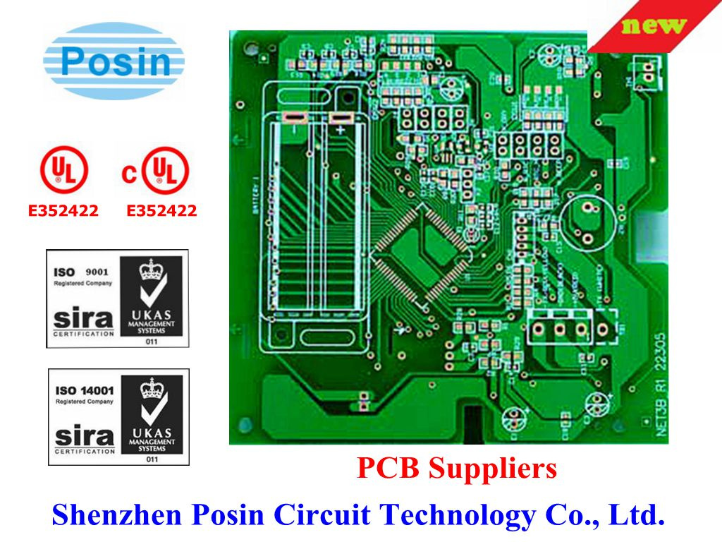
Product Specifications
| Prod Model: |
FABGerbers for ASRPS |
| Markets: |
North America,South America,Eastern Europe,Southeast Asia,Africa,Oceania,Mid East,Eastern Asia,Western Europe |
| Certificate: |
UL,ISO |
| Service: |
Prototype,PCBA,EMS |
| Type: |
Rigid Circuit Board |
| Dielectric: |
FR-4 |
| Material: |
Fiberglass Epoxy |
| Flame Retardant Properties: |
V0 |
Product Description
SpecificationsTechnologyNotes
Number of Layers0-32 Layers
Board Materials
FR4 (Tg 135C, 145C, 170C)
Rogers Ultralam 2000
Rogers RO4350
Rogers RO4003
Polyimide
Black FR4
Arlon AR350
Getek Copper Clad Thermal Substrates
Hybrid (Rogers and FR4) BT Epoxy
.
Stiffeners
Thermo Set and PSA Based Aluminum
FR4
Stainless Steel
Polymide
Core ThicknessMin. 0025"
Minimum Conductor Space0.003"
Minimum Conductor Width0.003"
Minimum Drill Hole Size0.006"
Finish Plating / Surface Finishes
HASL Leaded Solder Tin/Nickel
HASL Lead Free Solder
Electroless Soft Gold
Wire Bondable Soft Gold
Nickel Flash Gold
Electroless Nickel
Immersion Gold OSP
Electrolytic Nickel /Hard Gold and Selective Gold
Immersion Silver
Immersion Tin
Carbon Ink
ENIG
Finished Copper Outer Layers
1oz Cu Min. 004" Trace/Space
2oz Cu Min. 005" Trace Space
3oz Cu Min. 008" Trace/Space
4oz Cu Min. 010" Trace/Space
5oz Cu Min. 012" Trace/Space
We can manufacture higher ounces of copper depending on the specs. Please let us know how much you would like when sending us your PCB specs.
Finished Copper Inner Layers
. 5oz Cu Min. 004" Trace/Space
1oz Cu Min. 005" Trace/Space
2oz Cu Min. 006" Trace/Space
3oz Cu Min. 010" Trace/Space
4oz Cu Min. 012" Trace/Space
Inner Layer Clearances
Min. 008"
Minimum Finished Hole Size
Final Thickness <=. 062". 006' Hole Final Thickness. 150". 014" Hole
Final Thickness. 093". 010" Hole Final Thickness. 200". 018" Hole
Final Thickness. 125". 012" Hole Final Thickness. 250". 020" Hole
Gold Fingers1 to 4 edges
Silkscreen Type
Thermal Cure Epoxy Ink
LPI Ink
CNC Functions
Scoring Edge to Edge Plated Counter bores
Skip Scoring. 250" Spacing Milling
30 or 60 Degree Score Angle Blind and Buried Vias
30 to 100 Degree Countersink Controlled Z Axis Route
15 to 45 Degree Gold Finger Bevel Castellated Barrels
Counterbores Offset or Recessed Beveling
Plated Countersinks
Other PCB Services
Blind and Buried Vias
Plated Slots Specified Dielectric
Tented Vias Controlled Impedance
Solder mask Plugged Vias Via Caps (Solder Mask)
Conductive Filled Vias
Quality / Testing
Inspect to IPC Class III Continuity Resistance 10 to 20 Ohms
Net List Test per IPC-356D Isolation Resistance 2 to 30 Megaohms
Test Voltage 100 to 250 Volts Minimum SMT Pitch 0.5 mm
Tolerances
PTH Hole Size +/-. 002"
Front to Back +/-. 002"
NPTH Hole Size +/-. 001"
Solder Mask +/-. 002"
Tooling Holes +/-. 001"
Hole to Pad +/-. 005"
PCB industries / markets served
Military and Aerospace
Medical and Bio-medical
Industrial, Automotive, and Commercial:
Students and Hobbyist:
Shenzhen Posin Circuit Technology Co., Ltd. was established in April, 2008, After
years'efforts, the company has expanded rapidly and keptIntroducing
new production equipments. We have also trained a professional team
and perfected the quality management system ranging. the
manufacture ability of our company is expanded rapidly. The annual
output of double-sided and multi-layer PCB exceeds 100, 000
square meters.

